Address: 1/F, Building F, 5-6/F, West 4/F, Building E, Workshop Third(First), Zhoushi Road, Jiuwei, Bao'an, Shenzhen, Guangdong, China (M
Phone: +86-755-29991919
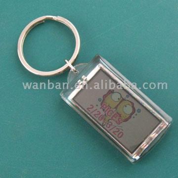
Solar Energy LED Key Buckle
The solar cell` s main principle is through the use of semiconducting material, andput the thinner model N semiconductor on the thick P semiconductor. When thephoton hitting the surface of this equipment, the adjoining plane of the model Pand model N semiconductor will create the electron scattering to produce the electriccurrent. The electric current can be stored up in the accumulator. It does notneed to replace the battery, and an touchable switch is available. Moreover, it isconvenient to take when in travel.Packing:Blister + paper cardIt can be designed by clients` demands
The solar cell` s main principle is through the use of semiconducting material, andput the thinner model N semiconductor on the thick P semiconductor. When thephoton hitting the surface of this equipm
The solar cell`s main principle is through the use of semi-conducting material, and put the thinner model N semiconductor on the thick P semiconductor, when the photon hiting the surface of this equip
The solar cell`s main principle is through the use of semi-conducting material, and put the thinner model N semiconductor on the thick P semiconductor, when the photon hiting the surface of this equip
The solar cell`s main principle is through the use of semi-conducting material, and put the thinner model N semiconductor on the thick P semiconductor, when the photon hiting the surface of this equip
Product Name: Solar LCD Key ChainModel Number: WBNS-033Place of Origin: ChinaBy using semiconducting material, and putting the thinner model N semiconductor onthe thick P semiconductor, when the photo
By using semiconducting material, and putting the thinner model N semiconductor onthe thick P semiconductor, when the photon hitting the surface of this equipment,the adjoining plane of the model P an
Product Name: Solar LCD Key ChainModel Number: WBNS-032Place of Origin: ChinaBy using semiconducting material, and putting the thinner model N semiconductor onthe thick P semiconductor, when the photo
By using semiconducting material, and putting the thinner model N semiconductoron the thick P semiconductor, when the photon hitting the surface of thisequipment, the adjoining plane of the model P an
By using semiconducting material, and putting the thinner model N semiconductoron the thick P semiconductor, when the photon hitting the surface of thisequipment, the adjoining plane of the model P an


 help
help Add to favorite
 Favorite products