Address: 1/F, Building F, 5-6/F, West 4/F, Building E, Workshop Third(First), Zhoushi Road, Jiuwei, Bao'an, Shenzhen, Guangdong, China (M
Phone: +86-755-29991919
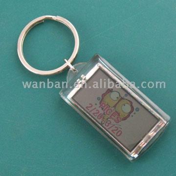
Solar LCD Key Chain
Product Name: Solar LCD Key ChainModel Number: WBNS-033Place of Origin: ChinaBy using semiconducting material, and putting the thinner model N semiconductor onthe thick P semiconductor, when the photon hitting the surface of this equipment,the adjoining plane of the model P and model N semiconductor will create theelectron scattering to produce the electric current. The electric current can bestored up in the accumulator. It does not need to replace the battery, and a touchableswitch is available. Moreover, it is convenient to take when traveling.Packing:Blister + paper cardCan be designed by clients
By using semiconducting material, and putting the thinner model N semiconductor onthe thick P semiconductor, when the photon hitting the surface of this equipment,the adjoining plane of the model P an
Product Name: Solar LCD Key ChainModel Number: WBNS-032Place of Origin: ChinaBy using semiconducting material, and putting the thinner model N semiconductor onthe thick P semiconductor, when the photo
By using semiconducting material, and putting the thinner model N semiconductoron the thick P semiconductor, when the photon hitting the surface of thisequipment, the adjoining plane of the model P an
By using semiconducting material, and putting the thinner model N semiconductoron the thick P semiconductor, when the photon hitting the surface of thisequipment, the adjoining plane of the model P an
By using semiconducting material, and putting the thinner model N semiconductor on the thick P semiconductor, when the photon hitting the surface of this equipment, the adjoining plane of the model P
By using semiconducting material, and putting the thinner model N semiconductor on the thick P semiconductor, when the photon hitting the surface of this equipment, the adjoining plane of the model P
By using semiconducting material, and putting the thinner model N semiconductoron the thick P semiconductor, when the photon hitting the surface of thisequipment, the adjoining plane of the model P an
The solar cell`s main principle is to semiconductor material, and put the thinner model N semiconductor on the thick P semiconductor, when the photon hits the surface of this equipment, the adjoining
The solar cell`s main principle is to semiconductor material, and put the thinner model N semiconductor on the thick P semiconductor, when the photon hits the surface of this equipment, the adjoining


 help
help Add to favorite
 Favorite products